Masoud Movahhedi, AbdolAli Abdipour Microwave/mm-wave & Wireless communication research Lab., Electrical Engineering Department, Amirkabir University of Technology, Tehran, Iran E-mail: Movahhedi@aut.ac.ir, Abdipour@aut.ac.ir
Abstract – A new wavelet-based simulation approach for the analysis and simulation of microwave/mm-wave transistors is presented. For the first time in the literature, Daubechies-base wavelet approach is applied to semiconductor equations to generate a nonuniform mesh. This allows forming fine and coarse grids in locations where variable solutions change rapidly and slowly, respectively. The procedure of nonuniform mesh generation is described in details by simulating a MESFET. It is shown that good accuracy can be achieved while compressing the number of unknown by 70%.’
Index Terms – full-wave analysis, nonuniform wavelet-base grid, transistor simulation, Daubechies-based wavelet.
I. Introduction
Recent progress in microwave technology over the past decade led to the development of smaller devices for higher operating frequencies. As the frequency increases, electromagnetic effect occurring inside the transistor cannot be neglected. Phenomena such as the phase velocity mismatch between gate and drain modes and reflection from electrodes open ends, affects the propagation of the wave along the device structure and therefore affects the device performance. Circuit-based models, distributed and semi-distributed models, usually used suffer from poor simulation of the EM wave propagation and questionable validity of the wave device interaction taking place inside the transistor [1]. The full- wave physical analysis of semiconductor devices is based on the coupling of Maxwell’s equations and the semiconductor equations used to characterize the dynamic of the electron inside the device [1]. After having an accurate device simulation approach, the characterization and full-wave analysis of microwave circuits included active and passive devices, is important. Therefore, the circuit analysis should be based on the advanced global model, which takes the electromagnetic (EM) wave effects into considerations. In the global modeling technique, the active devices are simulated by combining the electron transport and the EM models and the passive devices are simulated using the EM model [2].
The full-wave analysis of microwave and millimeter- wave transistors and global modeling of microwave circuits are a tremendous task that requires involved advanced numerical techniques and different algorithms
[3] . As a result, it is computationally expensive. Therefore, there is an urgent need to present a new approach to reduce the simulation time, while maintaining the same degree of accuracy. A conventional numerical approach to solve the differential equations of active part (transistors) and Maxwell’s equations for both passive and active parts is Finite-Difference Time-Domain (FDTD) technique. In this method, the unknown parameters are calculated in discrete positions named mesh nodes. By implementation a technique for generation a nonuniform mesh, we would considerably reduce the number of unknowns and also decrease the time of simulation and analysis. In this
This work has been supported in part by Iran Telecommunication Research Center (ITRS).
nonuniform mesh, the density of nodes in domains where the unknown quantities vary rapidly is higher than the other regions. Such a technique corresponds to a multiresolution of the problem. A very attractive way of implementing a multi-resolution analysis is to use wavelets [4]. Wavelets have been used in electromagnetics for a few years, first in the method of moments, and later in FDTD [5]. One of the approaches for solving Partial Differential Equations (PDEs) is the interpolating wavelets technique which has been applied to the drift-diffusion [6] and full hydrodynamic active device model [7].
In this paper, we propose to generate a nonuniform grid [8] for simulating of microwave transistors using Daubechies-based wavelet method. The transistor first is biased and steady-state parameter solutions are obtained using FDTD and uniform grid. Then, the proposed wavelet scheme is applied to the solutions and a nonuniform grid is generated. This mesh can be used in ac excitation state and decreases the time of full-wave simulation, significantly.
II.Daubechies-Based Wavelet Scheme
In the numerical simulation of equations it is common that small scale structure will exist in only a small percentage of the domain. If one chooses a uniform numerical grid fine enough to resolve the small scale features in the majority of the domain the solution to the equations will be over resolved. One would like, ideally, to have a dense grid where small scale structure exists and a sparse grid where the solution is composed only of large scale features. Now we consider a Daubechies-based wavelet system. Wavelets provide a natural mechanism for decomposing a solution into a set of coefficients which depend on scale and location. One can then work with the solution in a compressed form where one works only with the wavelet coefficients which are larger in magnitude than a given threshold. Wavelets, therefore, sound ideal for solving the type of problem mentioned previously
[8] .The idea of using wavelets to generate numerical grids began with the observation in [9] that the essence of an adaptive wavelet-Galerkin method is nothing more than a finite difference method with grid refinement. Jameson demonstrated in [8] that Daubechies wavelet expansion represents a localized mesh refinement. In this paper we will follow his wavelet based grid generation algorithm explained in [10].
III. Transistor Physical Model
The semiconductor models used are based on the moments of Boltzmann’s transport equations obtained by integration over the momentum space. Three equations need to be solved together with Poisson’s equation in order to get the quasi-static characteristics of the transistor. This system of coupled highly nonlinear partial differential equations contains current continuity, energy conservation and momentum conservation equations [11]. The solution of this system of partial differential equations represents the complete hydrodynamic model. Simplified models are obtained neglecting some terms in momentum equation. One of these simplified models is drift-diffusion model (DDM). In this paper we simulate MESFET as microwave/mm transistor that is a unipolar device. For this device, the equations to be solved in the drift-diffusion model are: Poisson’s equation: 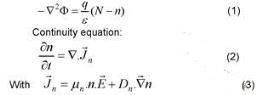
where® is potential, N is the doping profile, n is the electron (carrier) density, and /лп and D„ are the mobility and the diffusion coefficient, respectively. In this work, electron mobility has been considered as a function of doping and electric field:
The parameters of this equation have been defined in [12]. The diffusivity is defined by the Einstein relation D = kt/q/u.In order to characterize wave propagation-
device interaction inside the transistor, the electromagnetic and the semiconductor model must be coupled. The full-wave analysis and simulation start by obtaining the steady-state dc solution, using Poisson’s equation and the semiconductor device model. The dc solution is used in the ac analysis as initial values. Then the ac excitation is applied. Maxwell’s equations are solved for the electric and magnetic field distributions. The new fields are used in the semiconductor model to find the current density. This process is repeated for each time interval [1]. We use FDTD technique to solve the equations and achieve stable and accurate solutions. At the first, a uniform mesh that covers the 2-D cross section of the MESFET is used. Initially, the device is biased and the dc parameter distributions (potential and carrier density) are obtained by solving the drift-diffusion model only. After calculating the distributions of these parameters, we apply wavelet scheme to the solutions and determine where quantities vary rapidly and slowly. In domains that the variation of parameters is low, the wavelet method can refine the mesh and reduce the nodes of initial uniform mesh. By this method, we can generate a nonuniform mesh that its density is low in dispensable places. Because the dc solution is used in ac analysis as initial values and also the level of ac excitation is lower than dc level at most times, therefore one can conclude after applying ac excitation to the structure, the distributions of parameters will fix approximately. For this reason, we can use the nonuniform mesh generated from dc solution in ac analysis.
IV. Simulation Results
The approach presented in this paper is general and can be applied to any transistor. The transistor considered in this simulation is a 0.6-|im gate MESFET with the following dimensions and parameters: 1-|im-long source and drain electrodes, 0.7-|im source-gate gap, 1.5-цт gate drain separation, 0.2-|im-deep channel layer, and a
0. 8-|im-deep buffer or semi-insulating layer. Fig. 1 presents the conventional 2-D structure used for simulation. The doping of active layer is 1.2×10¹⁷ A/cm3 and the doping of the buffer layer is 1 x 10¹⁴ A/cm3. An 133 Дх x 33 Ay uniform mesh that covers the 2-D structure is used. Forward Euler is adopted as an explicit FD method to discretize drift-diffusion equations and Scharfetter- Gummel approximation [11] is used to determine the current density on the mid-points of the mesh. The device is biased to Vds = 2.0V and Vgs = -1V and the dc distributions of parameters are obtained by solving the physical model equations. The state of the MESFET under dc steady-state is represented by the distribution of potential and carrier density. Now, the mentioned wavelet approach is applied to each parameter (potential and carrier density) and then solutions are combined together to generate final nonuniform grid. Fig. 2 shows the procedure employed to obtain the nonuniform grid of the carrier density. The carrier density obtained from dc analysis is a function of x and y, n(x,y). The proposed wavelet scheme first, applies to the longitudinal cross sections, n(x), and removes some grids (Fig. 2(a)) and then applied to the transverse cross section, n(y), (Fig. 2(b)). The process is achieved by obtaining two separate grids for the transverse and longitudinal compressions. The two grids are then combined together using logical "AND” to conceive the overall grid for the carrier density (Fig. 2(c)). It should be observed that the proposed technique accurately removes grid point in the locations where variable solutions change very slowly (Fig. 2(d)). The same process is conducted for the other variable, potential. Fig. 3(a) shows the final grid for the potential after applying wavelet scheme. Because the variation of potential is slow, therefore the number of potential mesh nodes is smaller than the number of carrier density mesh nodes.
The separate grids of our variables are then combined using logical "OR” to obtain the overall grid for the cross section of MESFET (Fig. 3(b)). Considering the overall grid given by Fig. 3(b), the number of nodes after adding the necessary grid points is 1322, that shows about 70% compression for uniform mesh. The value of compression of algorithm depends on the threshold parameter defined in proposed wavelet scheme. In this simulation, threshold value has been set to 0.00008 for normalized quantities. One must trade off between the simulation time and solution accuracy to select the threshold value or level of compression. Now, this nonuniform mesh can be used to analyze the transistor when the ac excitation is applied. With this assumption that the level of ac excitation is lower than dc bias, the parameters distribution will be unchanged, approximately, and this nonuniform mesh will be valid. To evaluate of proposed method and generated nonuniform mesh, we added a gate voltage, Avgs = 0.1V, to the previous bias point and calculated drain current. The difference between the solutions, when uniform mesh and nonuniform mesh are used, equal to 2.9% that shows the accuracy of generated nonuniform mesh.
V. Conclusion
A wavelet approach based on the Daubechies wavelet scheme has been used to generate a nonuniform mesh toward full-wave analysis of microwave/mm-wave transistors. A reduction of 70% in the number of nodes is obtained while keeping drain current in an acceptable 2.9% of accuracy with the initial uniform mesh. This opens the door to an efficient numerical technique suitable for global modeling of microwave circuits.
[1]M. A. Alsunaidi, S. M. S. Imtiaz, and S. M. El-Ghazaly, "Electro-magnetic wave effects on microwave transistors using a full-wave high-frequency time-domain model,” IEEE Trans. Microwave Theory Tech, vol. 44, pp. 799-808, June1996.
[2]S. M. Sohel Imtiaz and S. M. El-Ghazaly, "Global modeling of millimeter-wave circuits: Electromagnetics simulation of amplifiers,” IEEE Trans. Microwave Theory Tech, vol. 45, pp. 2208-2216, Dec. 1997.
[3]R. O. Grondin, S. M. El-Ghazaly, and S. Goodnick, "A review of global modeling of charge transport in semiconductors and full-wave electromagnetics,” IEEE Trans. Microwave Theory Tech., vol. 47, pp. 817-829, June 1999.
[4]S. G. Mallat, "A theory for multiresolution signal decomposition: The wavelet representation,” IEEE Trans. Patt. Anal. Machine Intel!., vol. 11, pp. 674-693, July 1989.
[5]B. Z. Steinberg and Y. Leviatan, "On the use of wavelet expansions in the method of moments, "IEEE Trans. Antennas Propagat., vol. 41, pp. 610-619, May 1993.
[6]S. Goasguen, М. M. Tomeh, and S. M. El-Ghazaly, "Electromagnetic and semiconductor device simulation using interpolating wavelets,” IEEE Trans. Microwave Theory Tech., vol. 49, pp. 2258-2265, December 2001.
[7] Y. A. Hussein, and S. M. El-Ghazaly, "Extending multiresolution time-domain (MRTD) technique to the simulation of high-frequency active devices,” IEEE Trans. Microwave Theory Tech., vol. 51, pp. 1842-1851, July 2003.
[8] L. Jameson, "On the wavelet optimized Finite Difference method,” ICASE Report, No. 94-9, NASA Langley Research Center, Hampton, 1994.
[9] L. Jameson, "On the differentiation matrix for Daubechies- based wavelets on an interval,” ICASE Report, No. 93-94, NASA Langley Research Center, Hampton, 1993.
[10]L. Jameson, "Wavelet-based grid generation,” ICASE Report, No. 96-31, NASA Langley Research Center, Hampton, 1996.
[11 ] Y. K. Feng and A. Hintz, "Simulation of submicrometer GaAs MESFET Susing a full dynamic transport model,”
IEEE Trans. Electron Devices, vol. 35, pp. 1419-1431, Sept. 1988.
[12] X. Zhou and H. S. Tan, "Monte carlo formulation of field- dependent mobility for AlxGa^xAs,” Solid-State Electronics, vol. 38, pp. 567-569, 1994. 
Fig. 1. 2-D conventional structure of the simulated MESFET 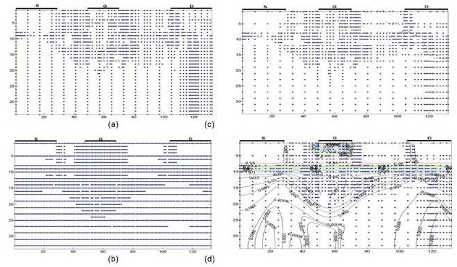
Fig. 2. (a) Compression for the carrier density at the longitudinal cross sections, (b) Compression for the carrier density at the transverse cross sections, (c) Final grid for the carrier density, (d) Normalized carrier density contour plot (n/Noi). 
Источник: Материалы Международной Крымской конференции «СВЧ-техника и телекоммуникационные технологии» |